

See Aurightec Insights, and Industry Insights
04
2018
-
12
Eolane China Fully Introduces DFM, Design for Manufacturing
Author:

DFM comes from the English abbreviation Design for manufacture. As the name implies, DFM fully considers the needs of manufacturing during the development of new products, so that the products have good manufacturability and reach the highest possible yield at the lowest cost in the shortest time.
In the traditional serial product development process, the design aspect always emphasizes the design progress, and focuses on the realization of product functions, and usually ignores the manufacturability of the product. This formed the "wall-to-wall design" of "we design, you make". In order to correct the manufacturing problems that occur in the sample trial production, multiple redesigns are required, and each improvement requires a re-production of the prototype, which is repeated and repeated until the design meets the production requirements, resulting in a long design cycle and serious delays. The time of product launch time greatly increases R&D costs.
DFM technology is an important part of DFX and is widely used in electronic design and electronic assembly manufacturing. The prominent role of DFM technology is:
Reduce product design modifications
Often the product is easily modified during the design phase and is difficult to modify during the manufacturing and assembly stages. Try to focus on the design modification in the product design stage, so that the manufacturability of the product is better, and the manufacturing and assembly of the product is relatively smooth.
Shorten product development cycle
One time through product verification compared to traditional product development, the development cycle is shortened and duplicate shots due to correcting manufacturing problems are reduced.
Reduce product costs
Focus design changes on the product design phase with the lowest design modification cost, simplify product design, reduce manufacturing process and assembly time, reduce product defect rate, and reduce cost waste.
Improve product quality
Through DFM design optimization, the product has been refined and optimized in the product design stage, which has good manufacturability and assemblability, reduces the number of quality problems in the post-manufacturing process, and improves the quality and reliability of the product.
The application of DFM technology in electronic design and electronic assembly manufacturing is mainly achieved through certain specifications and processes, supplemented by specialized tools. In order to assist customers in optimizing their designs and implementing a win-win model of "you design, we manufacture, design fully considers manufacturing needs" , Eolane China has invested in the Valor MPP software, a specialized tool for assisting DFM analysis. The software analyzes the matching of pins and pads by accessing the part database VPL to determine whether the best soldering effect can be achieved, thus achieving accurate assembly analysis. In addition, the software has built-in hundreds of rules (ERF), integrated industry specifications (IPC-7351, IPC-610-F, ...) and large manufacturing companies to conduct a comprehensive analysis of product design: including light plate size analysis, benchmarks Analysis, component spacing analysis, solder mask analysis, solder paste layer analysis, borehole layer analysis, and test point analysis. In addition, the software verifies the match between the BOM and the design. The software checks, measures and filters related design elements according to the built-in rules ERF, reducing the chance of human error and errors. It is worth mentioning that the application of VPL makes it easy to check the matching of the parts and pads.
Note: The VPL contains tens of millions of manufactured parts, each containing 3D data and part pin data.

The product design issues of a new energy customer described in the following case will bring process risks in the future production, and ultimately have different degrees of impact on product quality and cost. Eolane China proposed a corresponding solution through DFM analysis.
1. Pad design problem
Find the heel fillet value of 0 by using Valor software and report it. During further analysis, it was found that the distance between the two pads was relatively large, so that 28% of the solderable ends of the components did not touch the pads. Considering the dimensional tolerance of the solderable end is +/-0.25mm, the dimensional tolerance of the PCB pad is +/-20%, and the accuracy of the SMT placement machine is +/-0.1mm, and the open circuit occurs after reflow soldering. The possibility is relatively large. Once there is such a problem, manual repair is required. If the entire PCBA uses a certain package size of the device and the location of the repair is correspondingly large, it takes a lot of time, and ultimately will affect the product cost.
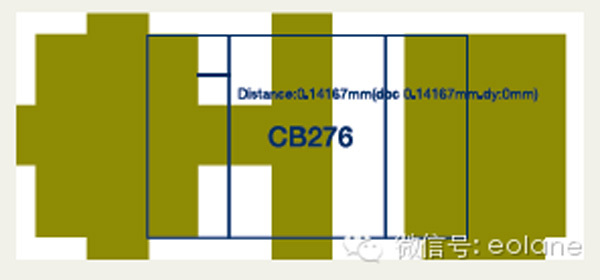
For this design, it is necessary to extend the pad inward from the DFM aspect to minimize the soldering problems caused by various factors.
Note: heel fillet is the distance from the innermost side of the pad to the solderable end of the part.
2. Tin hole design on the perforated component
The size of the tin hole is related to the tin effect. Under normal circumstances, thick plates, thick copper and grounding holes need relatively large holes, which allows more tin to pass through the holes without stopping the climbing due to heat dissipation. Finally, a better tinning height and a sufficient filling effect in the hole can be formed. In the DFM analysis, the plate thickness was found to be 2 mm, and the copper thickness of 2OZ was used, and some of the holes were small, and the distance between the hole and the component pins was 0.2 mm, and the plug hole was connected to the large copper surface. Therefore, the 0.2mm hole clearance is difficult to meet the 75% upper tin height requirement specified by IPC-610.
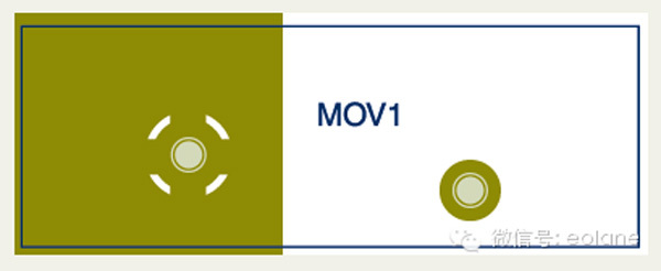
For this design, it is recommended to increase the aperture from the DFM aspect, improve the effect of tinning, and reduce the poor filling in the hole.
Key words:
Previous:
Next:
Previous:
Next:
Relate News
CONTACT
Add: Building 49, Dongjing Industrial Park, No.9 Dongfu Road, Suzhou Industrial Park, Jiangsu, China
Harry ZHOU
Tel: 86 138 1264 5838
Email: harry.zhou@aurightec.com

AURIGHTEC Group | AURIGHTEC China | LinkedIn | Facebook | Twitter | Youtube
Online message